
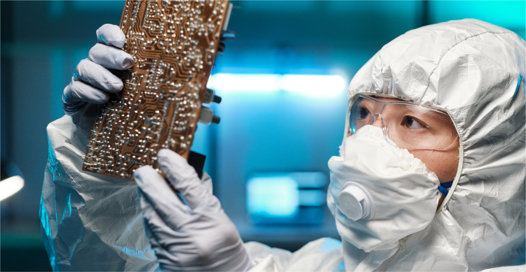

Telecommunications PCB Manufacturer
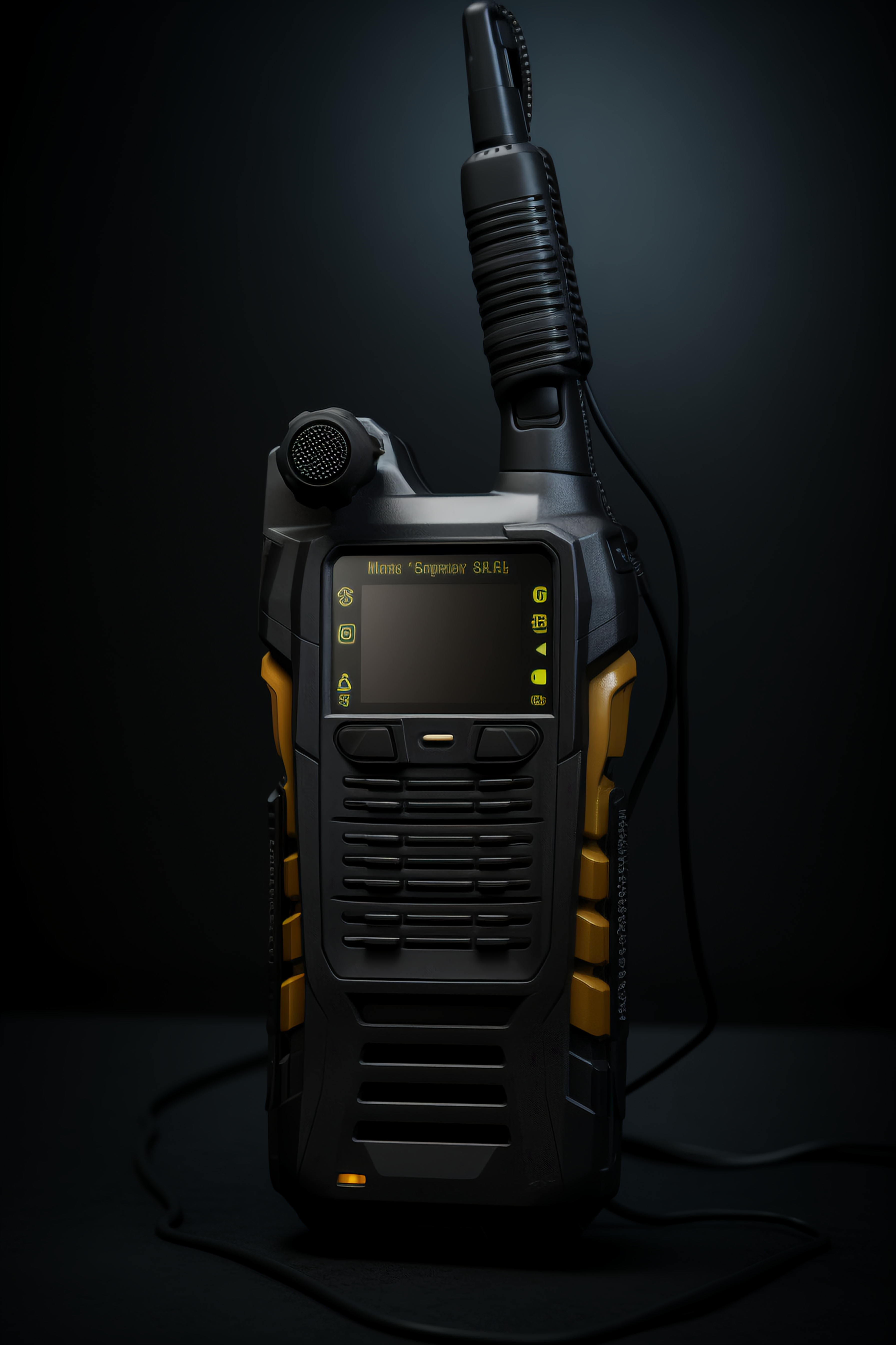
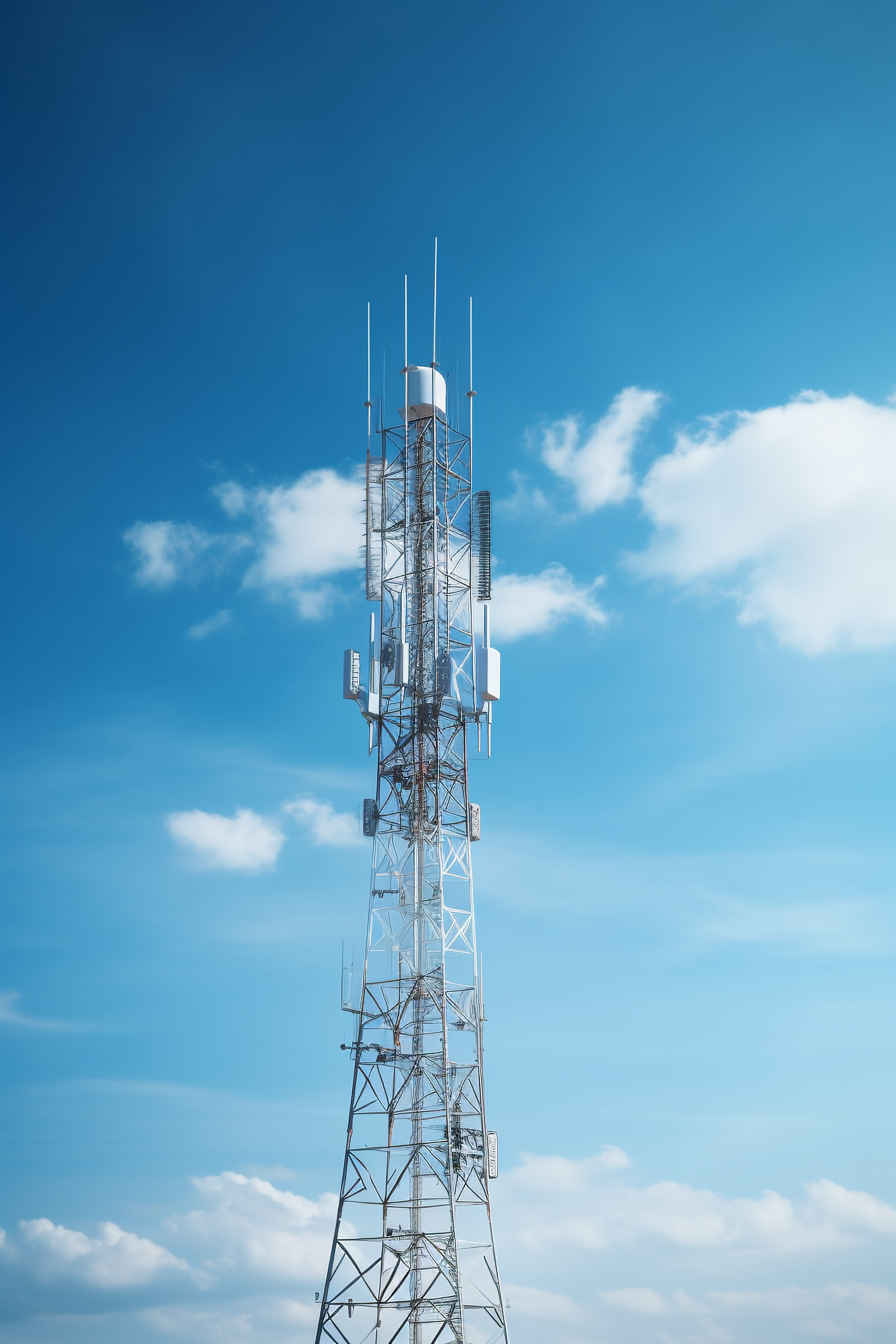
Telecommunication
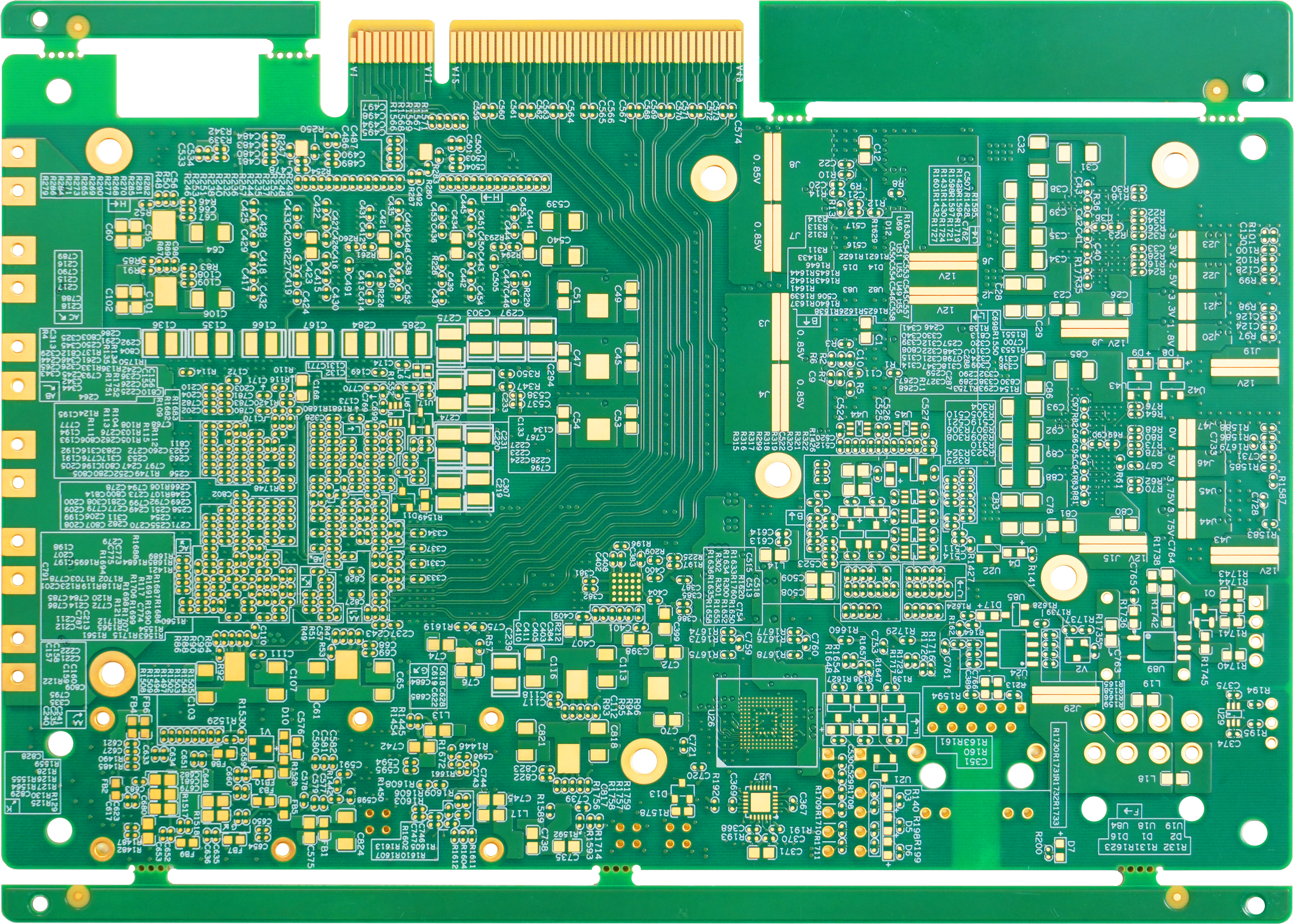
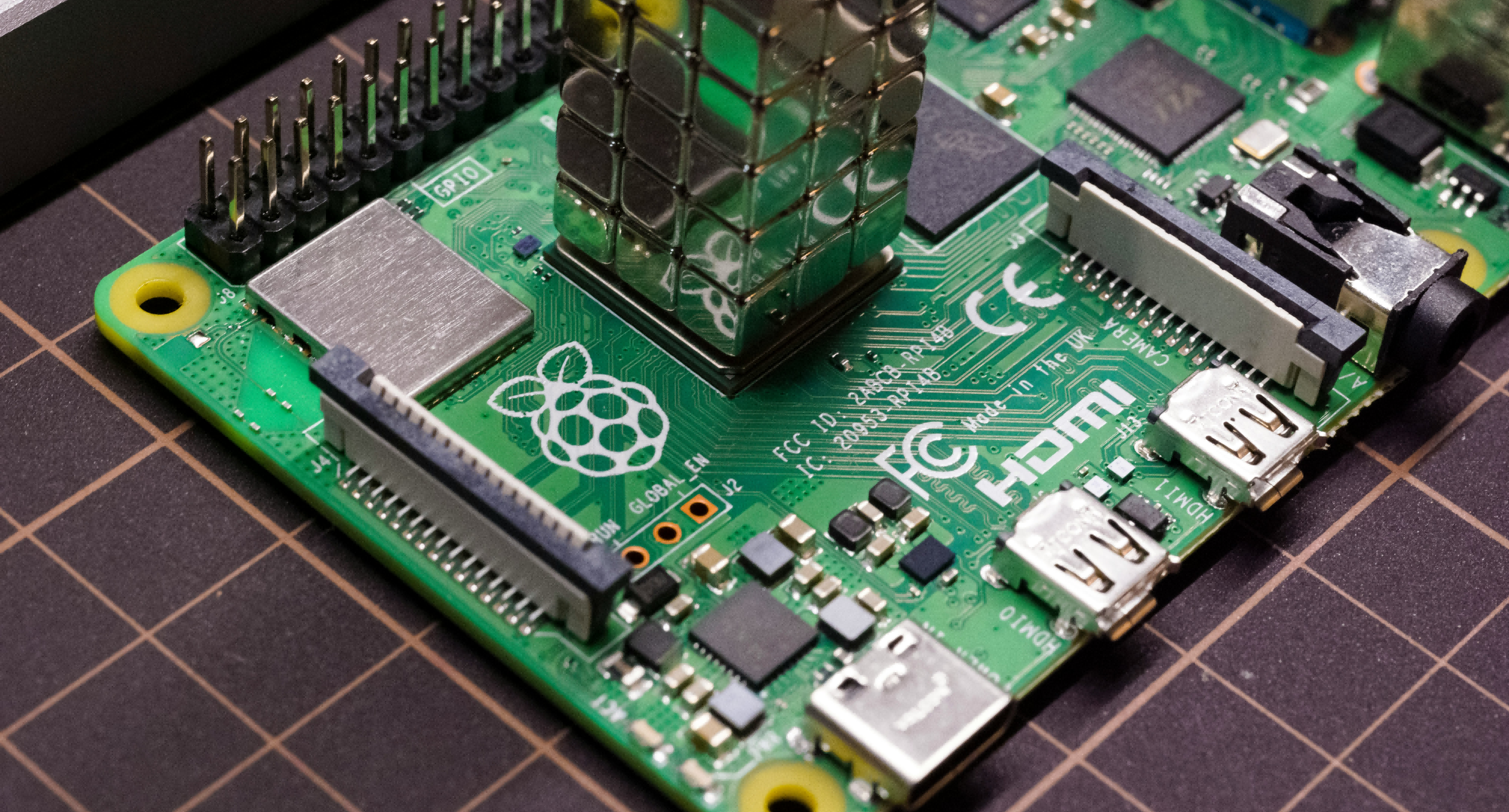
Printed Circuit Board
At KINGBROTHER, we are committed to collaborating with electronic device manufacturers from different industries to swiftly and efficiently bring innovative, high-tech products to market. We ensure the highest quality while strictly adhering to all regulatory standards.