
How to Make a PCB: PCB Manufacturing Process Guide
February 4, 2025


Printed circuit boards (PCBs) play an important role in directing current between electronic components. PCB manufacturing services cater to a wide range of applications, including industrial control systems (PLCs, HMIs, DCSs), automotive electronics, medical equipment (CT and MRI machines), and telecommunications equipment (routers and switches).
But what goes on in the manufacturing and design of PCBs? What materials and processes are used to bring PCBs to life? If you’re a new circuit designer within the PCB industry, read this article to learn more.
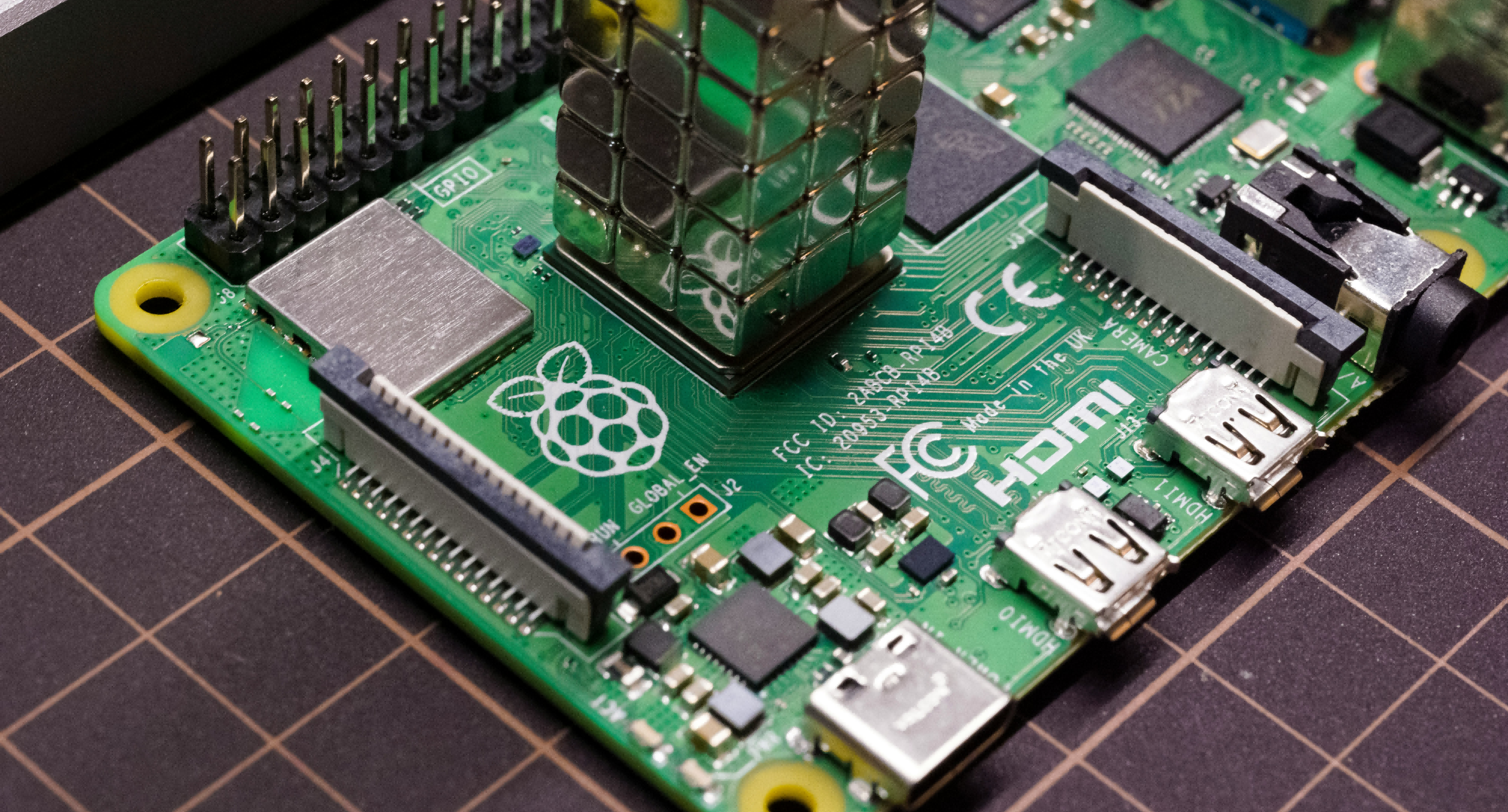
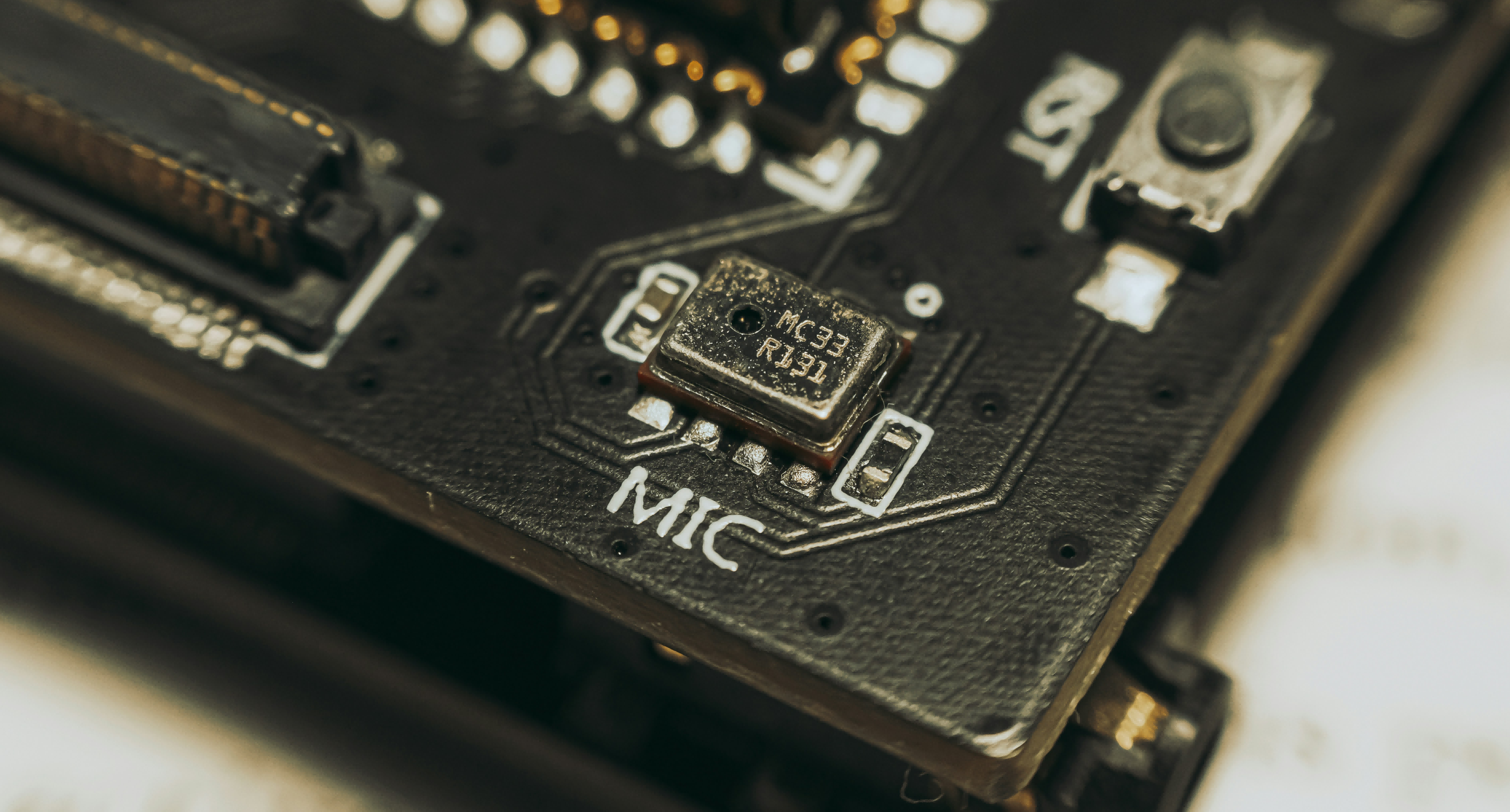
A PCB is an electronic assembly that uses copper conductors to connect electronic components. Besides that, the board also provides mechanical support for components when a device is mounted on an enclosure.
All PCB components connect via etched traces and vias. The overall structure is covered with a solder mask for insulation purposes and a silk screen that provides labeling for electronic components.
PCBs come in many different types with the most common being single-layer and multi-layer boards.
PCBs are the backbone of modern electronics, varying in complexity from simple single-layer boards to highly intricate multi-layer designs. Below, we explore their distinctions across manufacturing, cost, and application areas.
| Aspect | Single/Double-Layer Boards | Multi-Layer PCBs |
| Manufacturing Process | Involves basic steps with minimal complexity. | Complex and time-consuming due to bonding multiple layers and ensuring proper alignment. |
| Cost | Lower cost due to fewer materials usage and simpler assembly. | Higher cost due to advanced fabrication methods and additional materials. |
| Application Areas | Widely used in devices that require complex circuit designs, such as industrial control, and medical devices. | Primarily used in high-end electronic devices, such as industrial tablets, aerospace equipment, and high-precision medical instruments. |
The conductive layers that direct electrical current are made out of copper, while the substrate layers that provide insulation are made of fibreglass, commonly known as FR-4. Both layers are bonded with a type of adhesive known as an epoxy. Additionally, manufacturers may apply various coatings to protect PCBs against environmental damage.
PCB manufacturing process involves converting design files, which include Gerbers and netlists, into a physical circuit board on which components can be placed and soldered.
The fabrication process begins with design output files (Gerbers, netlist, drillfiles, etc). These output files are generated during the design phase, which includes developing a product concept, schematic entry, layout design, and file generation. The next stages include manufacturing and assembly of the board.
The flow chart below shows the steps involved in PCB manufacturing.

Prepare design files for PCB fabrication by converting them into manufacturing-ready formats.
Convert design files into Gerber or ODB++ format. Conduct Design for Manufacturing (DFM) checks, correct errors, and import files into the CAM system. Generate output files for drilling, imaging, solder masking, and routing.
Transfer circuit patterns onto the inner PCB layers.
Use Laser Direct Imaging (LDI) to print circuit patterns onto photoresist-coated panels.
Expose, develop, and remove unwanted photoresist to reveal the copper design.
Remove excess copper to create circuit patterns.
Employ chemical etching to dissolve unwanted copper and use AOI to ensure accuracy.
Remove residual photoresist to expose circuit patterns.
Dissolve and strip the photoresist using a chemical solution and high-pressure rinse.
Align and inspect layers for accuracy.
Use an optical punch machine for layer alignment and AOI for defect detection.
Protect copper and enhance bonding during lamination.
Apply a brown oxide coating to prevent oxidation and improve adhesion.
Bond multiple PCB layers into a single unit.
Stack layers and use controlled heat and pressure to laminate them.
Create holes for vias and components.
Drill holes using computer-controlled machines and deburr raised metal edges.
Make hole walls conductive for electrical connectivity.
Apply a thin copper layer to hole walls using chemical deposition.
Create circuit patterns on outer layers.
Clean panels, apply photoresist, and use LDI to print the outer layer design.
Enhance conductivity by plating copper on surfaces and holes.
Electroplate copper onto the PCB, followed by tin plating for corrosion protection.
Expose unwanted copper areas by removing photoresist.
Strip photoresist in a continuous process line.
Remove unwanted copper to finalize circuit patterns.
Use an ammoniacal etchant while tin plating protects essential copper.
Remove the protective tin layer.
Use nitric acid to strip tin without damaging copper circuits.
Protect traces and define solderable areas.
Apply and harden LPI solder mask, stripping unhardened areas.
Protect copper and enhance solderability.
Apply surface finishes like HASL, ENIG, or OSP.
Print labels and identification on the PCB.
Use manual silkscreening, inkjet printing, or laser etching.
Verify the PCB’s electrical functionality.
Perform Flying Probe or Bed of Nails testing to detect shorts and opens.
Ensure the PCB meets quality standards.
Conduct inspections, measurements, and functional tests.
Safely transport finished PCBs.
Boards are wrapped with ESD-safe materials and packed for shipment.
Typically, the manufacturing process of PCBs lasts between 3 to 20 working days. However, this duration can change depending on the quantity and type of PCBs ordered. When you need a board manufactured for prototyping or small-volume, KINGBROTHER is ready to deliver. Our consistent and reliable execution of quick-turn orders has earned us the trust and loyalty of our partners.
| Delivery | ||
| Layer | Lead Time | Quick-Turn Lead Time |
| 4 Layers | 6 Days | 3 Days |
| 6 Layers | 7 Days | 3 Days |
| 8 Layers | 8 Days | 4 Days |
| 10 Layers | 9 Days | 4 Days |
| ≥12 Layers | 16 Days | 5 Days |
The cost of manufacturing PCB can change depending on the types of materials and processes used. In particular, using FR-4 fibreglass is a much more economical option as they are compatible with standard manufacturing procedures.
On the other hand, polyimide, ceramic-based substrates and metal core materials require specialized machines and equipment to be processed into PCBs. This results in higher production costs. Before starting a PCB project, it is important to consider which materials and processes are required as well as their associated costs to avoid needless losses.
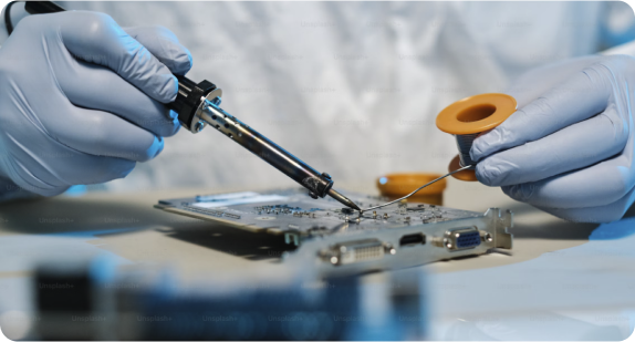
Getting each step of the PCB manufacturing process right is crucial as the component provides the foundation for connecting and supporting other electrical components. Producing PCBs involves a complex process that is costly. Therefore, companies often outsource to PCB manufacturers who have high levels of expertise and a long track record of creating high-quality PCBs for reputable brands.
Kingbrother has 28 years of experience in prototyping PCBs and providing quick-turn services. We specialize in custom-made PCBs that are tailored for a wide range of industries from automotive, health, and telecommunications.
If you’re looking to start a project, you can contact us to discuss details and requirements or visit our website for more information on our PCBs and other services.

