
Heavy Copper PCB: Applications, Benefits & Capabilities
July 9, 2025


When a Tesla Model S accelerates from 0-60 mph in under 3 seconds, its battery management system channels over 400 amps through specialized circuit boards. Standard PCBs would fail instantly under such extreme conditions, but heavy copper PCBs handle this challenge effortlessly.
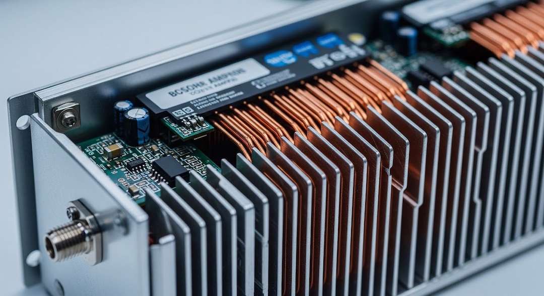
In today’s power-intensive applications, from electric vehicles to renewable energy systems, standard printed circuit boards simply can’t keep up. Heavy copper PCBs have emerged as the critical solution, featuring copper layers up to 10 times thicker than conventional boards. These specialized circuits enable higher current loads, superior thermal management, and enhanced reliability across demanding industries.
This comprehensive guide explores PCB heavy copper device technology and demonstrates how KINGBROTHER’s 28+ years of expertise deliver cutting-edge solutions for the most challenging applications.
Heavy copper PCBs are printed circuit boards featuring copper weights of 3 ounces per square foot (3 OZ) or greater—a large increase from standard PCBs that typically use 0.5 OZ to 2 OZ copper. Some extreme applications require copper weights exceeding 20 OZ.
The PCB heavy copper weight system measures how much copper foil would weigh when spread over one square foot. Each ounce correlates directly to thickness: 1 OZ = approximately 1.4 mils (0.0014 inches).
| Features | Standard | Heavy |
| Weight | 1 OZ – 2 OZ | 3 OZ – 20 OZ+ |
| Thickness | 1.4 – 2.8 mils | 4.2 mils+ |
| Applications | Consumer electronics, digital circuits | Power electronics, industrial systems, and automotive |
| Current Capacity | Limited | 5-10x higher |
Choose heavy copper PCBs when your application requires:
Heavy copper PCB manufacturers primarily use two types, each optimized for different applications:
How it’s made: Applied through electroplating processes during PCB fabrication.
Key characteristics:
Best for: Applications where mechanical stress resistance is critical and cost-effectiveness matters
How it’s made: Mechanically rolled to precise thickness specifications.
Key characteristics:
Best for: High-frequency applications and circuits requiring superior electrical characteristics
At KINGBROTHER, we can work with you to select the optimal copper type based on your specific application requirements, performance goals, and budget considerations.
Copper thickness in PCBs follows industry-standard measurements:
KINGBROTHER’s Capabilities: Up to 18 OZ copper thickness for prototyping and 6 OZ for mass production, positioning us to handle the most demanding heavy copper requirements across industries.
Successfully implementing heavy copper PCBs requires careful attention to several critical design factors:
Heavy copper PCBs excel at thermal management due to copper’s superior thermal conductivity (401 W/m·K). Key design considerations include:
The current-carrying capacity increases significantly with copper thickness:
PCB heavy copper electronic designs require specialized stack-up planning:
Heavy copper board for PCB presents unique challenges for via formation:
Understanding these design considerations is crucial for successful heavy copper PCB implementation. When properly designed and manufactured, heavy copper PCBs deliver performance advantages that make them indispensable for demanding applications.
Heavy copper PCBs deliver five critical advantages that make them essential for power-intensive applications:
Heavy copper conductors handle 5-10 times more current than standard traces. A 3 OZ copper trace can safely carry approximately 3x the current of a 1 OZ trace, enabling high-power applications previously impossible with standard PCBs.
Copper’s exceptional thermal conductivity becomes a major advantage in heavy copper PCBs. The increased copper mass creates effective heat spreading pathways, reducing component temperatures by up to 50% and greatly improving system reliability.
Lower resistance paths minimize I²R losses, improving overall system efficiency. In high-current applications, this translates to significant energy savings and reduced heat generation, critical for battery-powered and energy-conscious designs.
Thicker layers within a heavy copper PCB 4-layer provide enhanced mechanical stability and superior resistance to thermal cycling stress. This durability is essential for applications experiencing temperature fluctuations or mechanical vibration.
Heavy copper reduces ground bounce and provides improved power distribution, enhancing signal quality in high-current circuits. This benefit is particularly valuable in mixed-signal designs combining power and sensitive analog circuits.
These compelling advantages explain why heavy copper PCBs have become essential across multiple industries. From renewable energy to medical devices, let’s examine how different sectors leverage heavy copper technology to solve their most challenging problems.
The renewable energy revolution has created unprecedented demand for efficient power conversion systems. Heavy copper PCBs serve as the backbone of this transformation.
Critical Applications:
Why KINGBROTHER? Our power industry expertise, combined with up to 18 OZ copper capabilities, enables energy system manufacturers to achieve maximum efficiency and reliability. We understand the unique thermal and electrical challenges of renewable energy applications.
In medical applications, reliability isn’t just important — it’s literally a matter of life and death. Heavy copper PCBs provide the robust foundation that critical medical devices require.
Mission-Critical Applications:

KINGBROTHER’s Medical Advantage: With ISO 13485 certification and deep medical device expertise, we deliver heavy copper solutions that meet the most stringent regulatory requirements while maintaining the reliability healthcare demands.
Modern manufacturing relies on increasingly sophisticated automation systems that demand robust, high-power electronics capable of operating reliably in harsh industrial environments.
Essential Applications:
Industrial-Grade Reliability: KINGBROTHER’s industrial control expertise ensures heavy copper PCBs meet demanding factory automation requirements, from automotive assembly lines to chemical processing plants.
The rollout of 5G networks and expanding telecommunications infrastructure creates new demands for high-power, thermally efficient circuit boards.
Next-Generation Applications:
 Telecom Expertise: KINGBROTHER’s telecommunications experience enables optimal heavy copper solutions that meet the demanding requirements of modern communication infrastructure.
Artificial intelligence and IoT devices are pushing the boundaries of computational power while demanding compact, thermally efficient designs.
Emerging Applications:
Future-Ready Solutions: As AI and IoT markets continue expanding rapidly, KINGBROTHER’s heavy copper capabilities address the next generation of power and thermal management requirements.
KINGBROTHER stands out amongst other heavy copper PCB suppliers through:
From electric vehicle powertrains to renewable energy systems, heavy copper PCBs enable the high-performance applications shaping our future. With current-carrying capacity up to 10x standard PCBs, superior thermal management, and enhanced reliability, heavy copper technology transforms challenging design requirements into achievable solutions.
Ready to harness heavy copper power? Contact us now to discuss your specific heavy copper requirements.

