


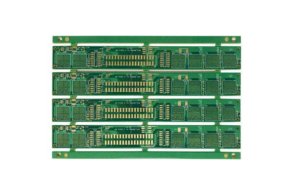
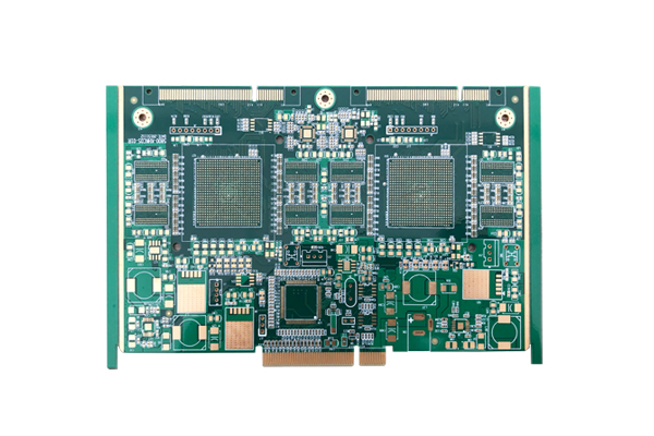
| With 20+ years of experience on PCB prototyping and quick-turn services, KINGBROTHER has built an agile manufacturing system, especially for high-mix low-volume orders to shorten R&D period of customers. |
 |
Key Features |
|
Multi-layer |
|
|
|
1.Up to
64 layers; |

|
|
Rigid-Flex |
|
|
1.Metal-plated holes and PTH Pad on
FPC can realize build-buried
holes connecting and soldering; |

|
HDI |
|
|
|
1.Multi-step
HDI enables the connection between any layers; |
|
|
High Frequency / Microwave |
|
|
1.Multi-layer
PTFE laminating enables super high frequency PCB; |

|
Metal Core / Metal Base |
|
|
|
1.Multi
laminating aluminum-based PCBs / Soldering technology to
cooper-base PCBs fulfill the needs of better heat radiating
on multi-layer PCBs; |

|
|
High Speed Signal Transmission |
|
|
1.Capable
to process the 56Gbps high-speed back panels and 100Gbps
high-speed optical modules; |
|
Others |
|
|
|
1.Embedding
technology fulfills the needs of integrated structure inside
PCB to embed magnetic cores, daughter PCBs, metal cores, and
components; |

 |
Characteristics and Advantages |
|
Key Technology |
Qualified Suppliers | |
|
Professional R&D on high density HDI, multi-layer PCB, rigid-flex PCB, embedding technology of small size core, thick GEM, PCB with special requirements from industries like defense / medical / automotive, and others technologies. |
Sourcing from Rogers, Shengyi,Wazam, Dupont, Rohmhass, Atotech and other excellent suppliers. |
|
Quality Certificates |
Footprints | |
|
ISO standard quality system certificates, high standard environmental-friendly production. |
3 agile manufacturing plants and 18 service centers. |
|
Delivery |
|||||||||||||||||||||||||||||||||
|
Prototyping Lead Time (<1㎡) |
|||||||||||||||||||||||||||||||||
|
|
Mass Production Lead Time |
|||||||||||||||||||||||||||||||||||||||||||||||||||||||||||||||||||||||||||||
|
|||||||||||||||||||||||||||||||||||||||||||||||||||||||||||||||||||||||||||||
 |
Quality Guarantee |
| KINGBROTHER serves for a wide range of industries with mature quality system certificated with ISO9001/ISO14001.With our quality assurance process and management tools e.g.SPC, MSA, FMEA, APQP and PPAP, KINGBROTHER could both ensure the quality and delivery following a wide range of features and requirements from 15000+ R&D customers. All of our PCB will go through 100% E-testing and AQI checking and could also go through various testing for reliability including high voltage, high-low temperature, impedance control, micro-section, solderability, thermal stressing, isolated resistor, ionic contamination and else. |
 |
Application |
|
AI, Telecom, Industrial control, Medical, Electricity, Automotive, PCs. |
|
 |
Capability |
|
Max 64L, ±1.0mil tolerance control for line, min 0.1mm drill bit. |
|
 |
Equipment |
|
Mitsubishi, Burkle, Orbotech, Tek… |
|